

It has been about two months since my first post regarding the Xserve RAID ("XR"). Since then, I have explored the caddy design in greater detail, including the PCB discussed in the earlier post, the geometry of the caddy itself, and potential options for a SATA backplane. While the latter two topics will be discussed in forthcoming posts, this post will again focus on the PCB included in every non-blank caddy. Oh, and I've decided to call the (hopefully inevitable) fruit of this project the "Xsata." Cool.
I think one of the goals of this project will be to mangle as little of the original XR as possible. That said, the chassis will likely be on the receiving end of some more destructive modifications (thanks, rivets). For... some reason, I guess? Though I am pretty sure that most (if not all) of the soon-to-be-redundant parts will likely be never used again.
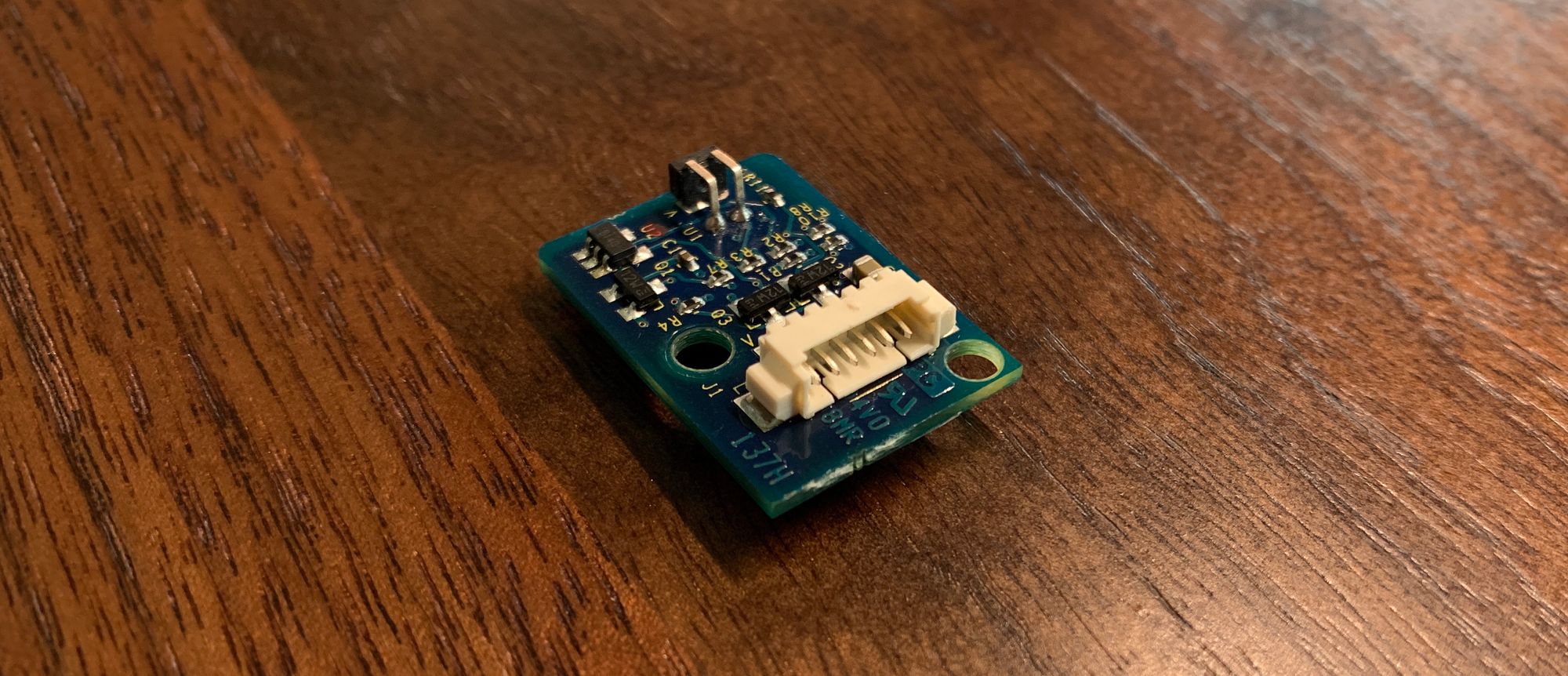
In that vein, I started by ordering a new "cable assembly" that fits the 6-pin header on the PCB (above). That way, the original connector (and associated SCSI PCB) can remain intact. It is probably also worth noting that the housing and leads could have each been ordered separately and then assembled, which would likely have been more cost effective at the expense of my time and patience.
Anyways. Once I had the cable assemblies in-hand, evaluating the PCB was much easier. I started by soldering the leads from the caddy PCB to the pads of a test backplane PCB, as I laid out in my earlier blog post:
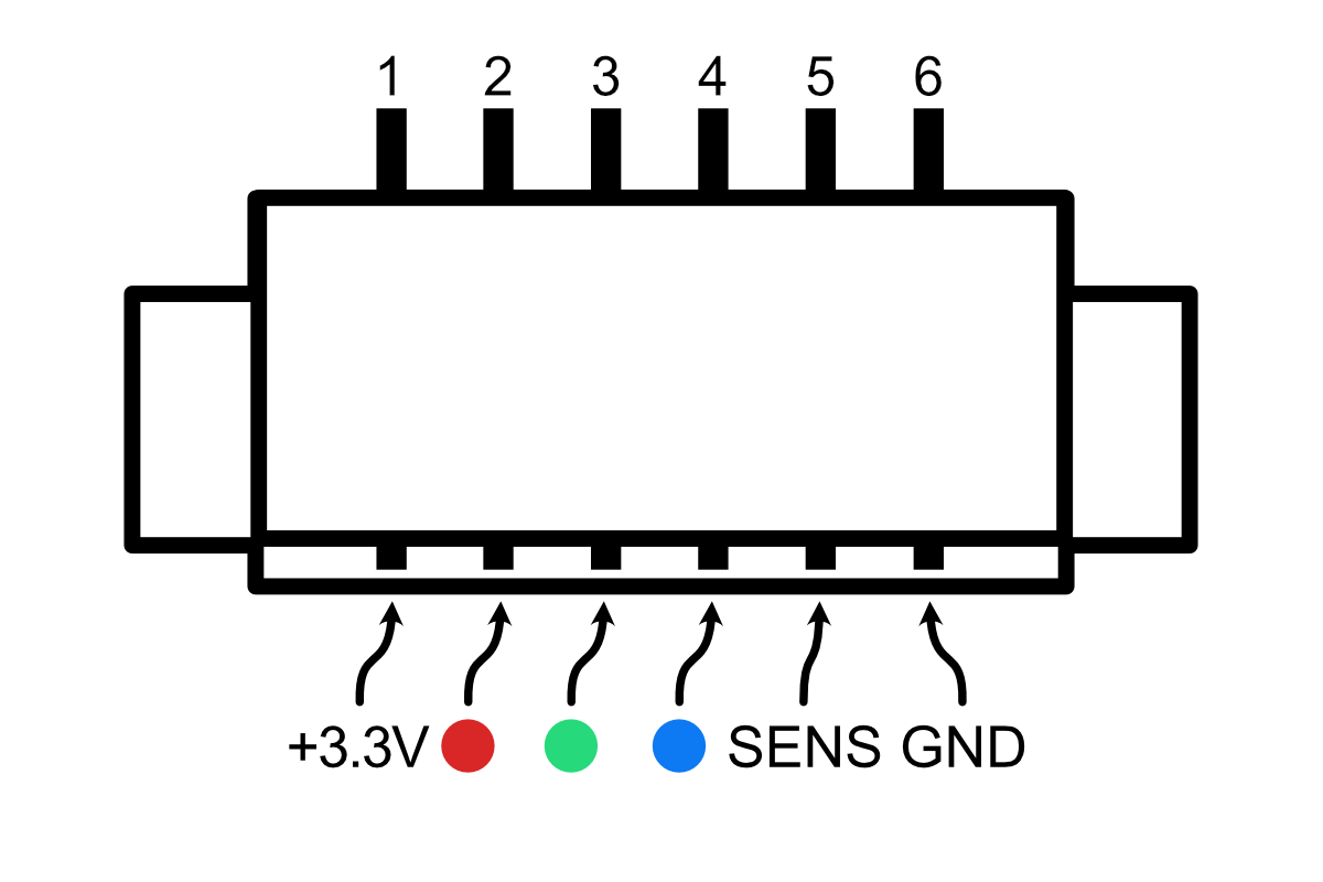
So, my plan will be to find a backplane PCB with activity and power leads / LEDs, so I can wire pins 1, 3, and 6 for power (i.e., yielding a green color on the status LED of the caddy) and pin 4 (and pin 6) for disk activity.
~me, 2021.05.10
Boy, I made it sound so easy. The status/power LED lit up with seemingly no problems. Unfortunately, so did the activity LED, which is to say that both LEDs stayed lit. Not only that, the caddy PCB also became very hot to the touch shortly thereafter. Just super.
Turns out the caddy PCB isn't used to 5V. After some testing and additional research (SCSI operated at 15V and 3.3V, instead of SATA's 12V and 5V), it seems that 3.3V likely makes more sense. I have since updated the earlier blog post to include this discovery.
Now is probably as good a time as any to mention my total lack of experience with circuits. I was supposed to take a class on circuits in college and, yet, I didn't. So this project was coming along exactly as expected.
I initially considered a voltage divider as a potential solution to drop 5V to 3.3V, but settled on a linear voltage regulator for fear that the input voltage and output current draw may not be reliable/constant.
Failings of yours truly aside, the activity LED was still a problem. I had expected the SATA PCB to signal using the positive pad rather than the negative pad. This wouldn't be a problem if the LEDs of the caddy PCB didn't share a common ground lead. But they do!
I thought this was an oddity of the SATA PCB that I was using, but, in actuality, it appears this is part of the SATA power connector. Enter: pin 11. Per Wikipedia, pins 1-3 are 3.3v (if you're into shucking HDDs, you may be familiar with pin 3), pins 5-6, 10, and 12 are ground, pins 7-9 are +5V, and pins 13-15 are +12V. Pin 11, however, is described as follows:
Pin 11 can function for staggered spinup, activity indication, both, or nothing. It is an open-collector signal, which may be pulled down by the connector or the drive. If pulled down at the connector (as it is on most cable-style SATA power connectors), the drive spins up as soon as power is applied. If left floating, the drive waits until it is spoken to. This prevents many drives from spinning up simultaneously, which might draw too much power. The pin is also pulled low by the drive to indicate drive activity. This may be used to give feedback to the user through an LED.
~Wikipedia, Serial ATA § Standard Connector (emphasis mine)
Based on my incredibly limited understanding, I took this to mean that pin 11 may be left floating, until it is pulled low by the drive to indicate activity. Super helpful; that explained the unexpected-to-me behavior of the "Activity –" pad on the SATA PCB.
Armed with knowledge and a renewed sense of give-a-fuck-edness, I broke out my super shitty breadboard, 5V power source (USB: putting the "U" in "USB" since 1996), 3.3V linear voltage regulator, resistors, transistors, and, eventually, MOSFETs. Behold the resulting circuit:
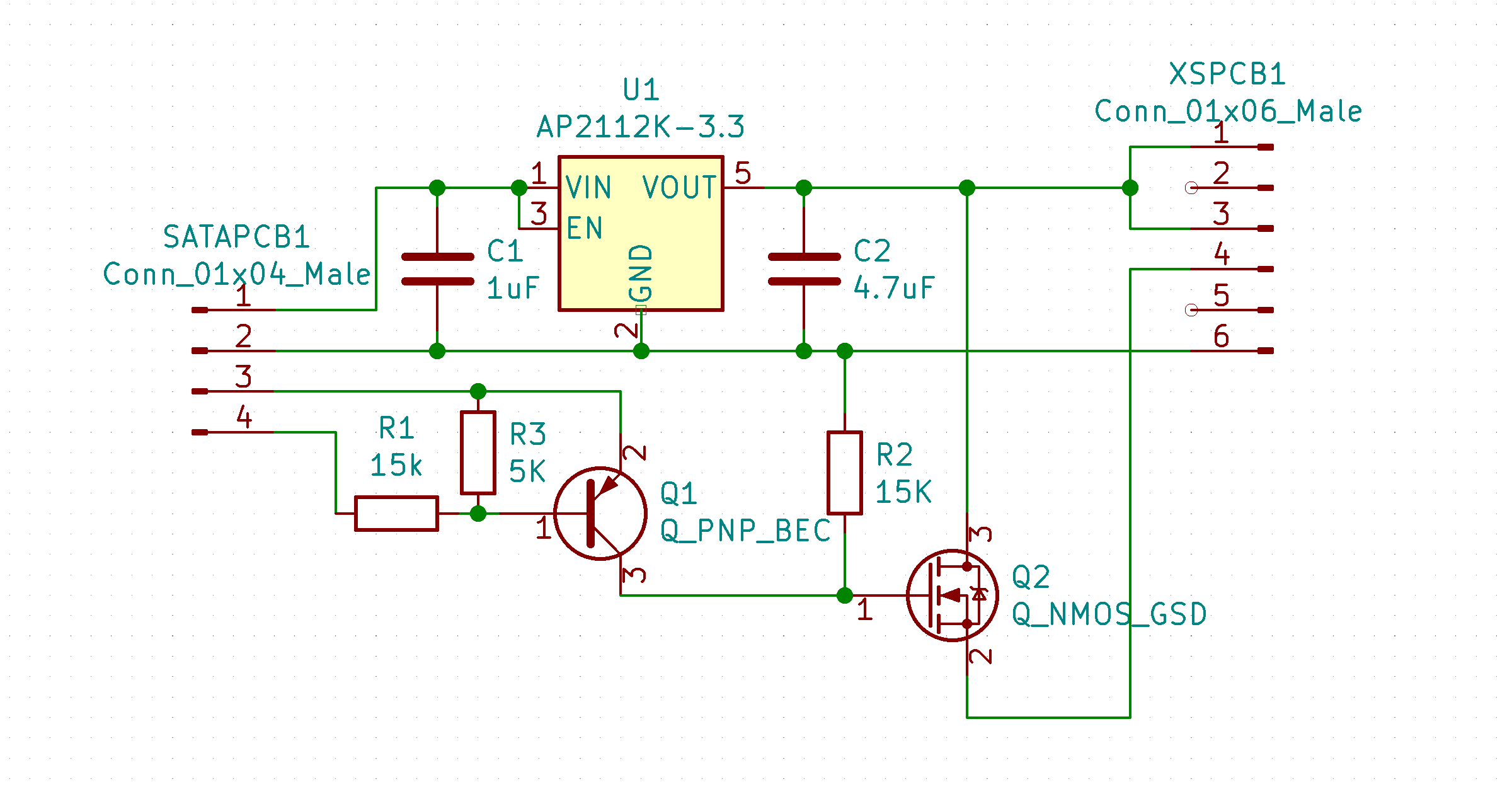
It's been a multi-week process at this point, so I am a little foggy on the details (read: past failures), but the ultimate design uses a PNP transistor (Q1) in combination with an n-channel MOSFET (Q2) to control the Activity LED (and, more specifically, to conditionally provide +3.3V from the voltage regulator (U1) to pin 4 of the caddy PCB).
It will be more soldering than I had wanted to do (especially when I have to do it for each caddy–14 times over), but let's walk through each of the components and why they're there.
To start, the left connector is intended to connect to the SATA PCB, where pad 1 = power +, pad 2 = power –, pad 3 = activity +, and pad 4 = activity –. The caddy PCB is on the right, where pins 1 and 3 provide +3.3V to the power LED, pin 4 provides +3.3V to the activity LED, and pin 6 is ground.
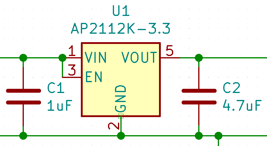
Moving to the middle of the schematic, the top portion (enlarged above) is easiest to explain. U1 is a 3.3V linear voltage regulator, where pin 1 is VIN (i.e., +5V from pin 1 of the SATA PCB connector), pin 2 in GND (i.e., ground from pin 2 of the SATA PCB connector), pin 3 is the enable pin (which, per the spec sheet, is pulled high to enable the regulator), pin 4 is unused, and pin 5 is VOUT (i.e., +3.3V to one or both caddy PCB LEDs).
C1 (1µF) and C2 (4.7µF) are capacitors that smooth the input to and output from the voltage regulator, respectively. I can't take credit for the inclusion and values of C1 and C2; the spec sheet recommended their inclusion for improved stability.
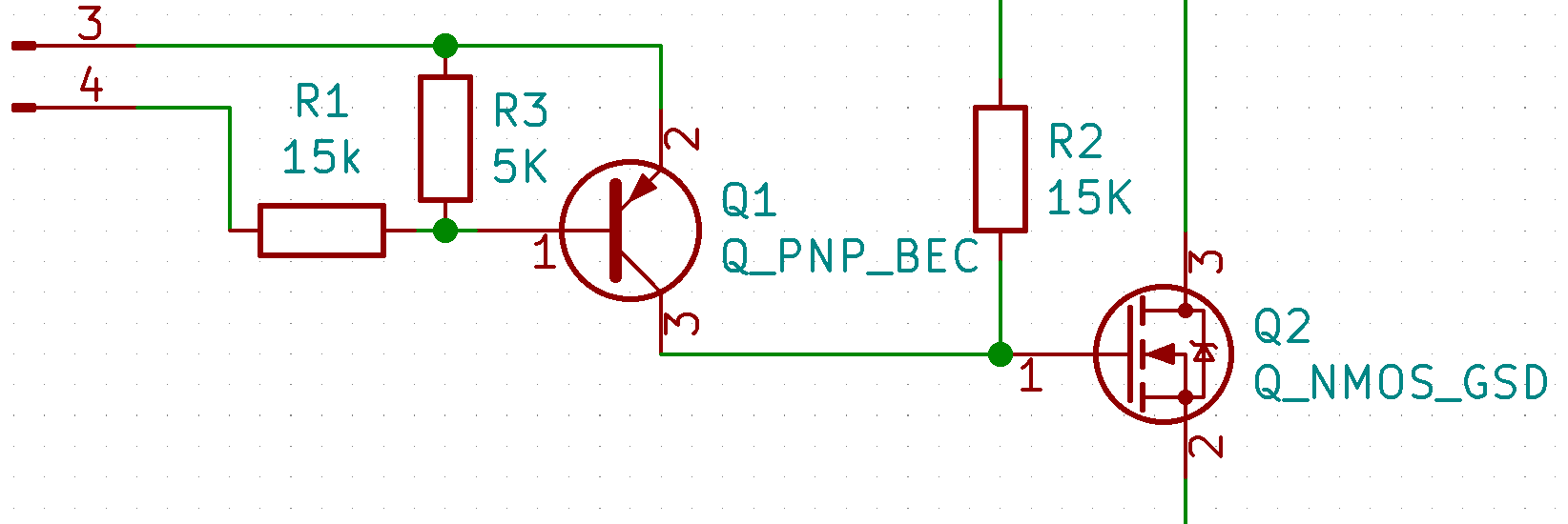
Let's turn now to the bottom portion of the schematic (reproduced above). At its core, Q1 controls the gate of the MOSFET (i.e., pin 1 of Q2), thereby causing electricity to flow from the linear regulator to the activity LED (i.e., from the drain, pin 3, of Q1 to the source, pin 2) when current flows from pin 2 to pin 1 of the PNP transistor (Q1). Put another way, when current flows from pin 2 to pin 1 of Q1 (as a result of a drive pulling pin 4 of the illustrated connector low), Q1 is "on," such that the voltage at the gate of Q2 is +5V. As a result, Q2 is "on" too, thereby causing the activity LED to be illuminated.
With respect to the resistors, R1 limits the current passing through Q1 (as well as R3). R3 is a pull-up resistor, which causes the emitter (pin 2) and the base (pin 1) of Q1 to have a similar voltage so Q1 is not "on" when pin 4 of the SATA PCB connector (i.e., pin 11 of the SATA power connector, as discussed above) is floating.
It is not visible in the excerpt above, but R2 is a pull-down resistor (connecting the gate, a.k.a. pin 1, of Q2 to power –, or ground). This ensures that, unless Q1 is "on," Q2 does not receive a sufficient positive voltage to itself be "on." The values of R1, R2, and R3 were determined experimentally using my breadboard and are deliberately high values in an effort to reduce wasted current. These values may change in the final design, but at least resistors are cheap.
I have also designed and ordered a batch of PCBs based on the above schematic, but that is the topic for a future post; this one is long enough. Hopefully I will have the PCBs in hand soon (and determine that the design works), at which point I will add another post to the growing Xsata saga (hmm, perhaps this is the Xsaga?). Fingers crossed.